Do you want to attend FREE Bootcamp of IT courses?
Edit
I am a Student Faculty
Our councellor will reach back to you on your preffered time slot to help you make a better decision.
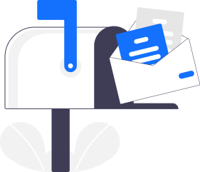
Our counselor will get back soon to help you make a better decision.
Our experts can answer your questions
Your test is submitted successfully. Our team will verify you test and update in email for result.